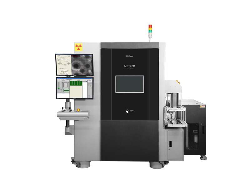
X-eye NF120
Nano-focus X-ray
-
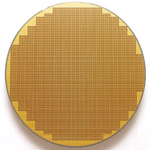
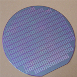
Non-destructive analysis system for Wafer Level Packaging
-
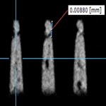
High resolution image with Dual Type CTs
-
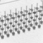
TSV, Micro Bump, Pattern
|
Nano-focus X-ray Inspection System |
Specifications
| X-ray Tube | 120 kV / 200 µA |
|---|---|
| Min. Resolution | 0.2㎛ |
| Table Size | 12inch wafer |
| Detector | 6 inch FPXD |
| CT Scan Method | Oblique CT / Cone beam CT |
| Foot print | 2,380 x 1,450 x 2,120 mm Control Box : 600 x 1,250 x 1,030 mm |
| Weight | 7,000kg |
| AXIS | X, Y, Z, Tilt (70º), R |
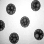
Wafer Bump Void
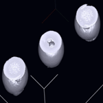
Wafer TSV Void